Title: Graphene Band Structure Tailoring by Superperiodicities and Nanostructuration.
When: Tuesday, March 12, (2019), 12:00.
Place: Department of Condensed Matter Physics, Faculty of Sciences, Module 3, Seminar Room (5th Floor).
Speaker: Antonio Tejeda, Laboratoire de Physique des Solides, Université Paris-Sud, CNRS, France.
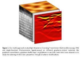
The disadvantage of graphene for using digital electronics is lack of bandgap, which is necessary to perform on-off switching operations in transistors. We have shown three different approaches to open a gap in graphene and tailor its electronic band structure. This includes [1] nanostructuration of graphene into graphene nanoribbons, [2] preparing a well-ordered buffer layer graphene and [3] introduction of a superperiodic potential in graphene grown on vicinal noble metal substrates. In our first approach to control graphene band structure, we have considered graphene ribbons grown on facets of the SiC(0001) surface [1,2]. Our morphological characterization by scanning tunneling microscope (STM) and cross sectional transmission electron microscope (TEM) shows the presence mini-ribbons bordering a central extended ribbon. These mini-ribbons have a width of 1-2 nm and promote an electronic confinement gap of more than 0.5 eV as observed by photoemission, in an otherwise decoupled graphene from the substrate [3,4]. We have also studied the first stages of graphene growth. On SiC(0001) substrate, under adequate growth conditions, a well ordered first single layer graphene (i.e. the buffer layer) exhibits again a bandgap of more than 0.5eV [5]. The origin of this bandgap was unclear, so we used STM, TEM angle-resolved photoemission spectroscopy (ARPES) together with calculations. This comprehensive study demonstrated that the bandgap opening is due to the super periodicity induced by the substrate [6,7].
Finally, we induced different superperiodicities on the underlying substrate to tailor graphene’s electronic properties. The nanostructuration of two substrates, Ir(332) and a multivicinal curved Pt(111) substrate induces a superperiodic potential on graphene that opens mini-gaps on the π band as observed by ARPES and consistent with the structural periodicity observed in STM and low energy electron diffraction [8].
References
Universidad Autónoma de Madrid © 2008 · Ciudad Universitaria de Cantoblanco · 28049 Madrid · Información y Conserjería: 91 497 43 31 E-mail: informacion.ciencias@uam.es Gestión de estudiantes de Grado y Posgrado: 91 497 8264 / 4329 / 4353 / 4349 / 6879 / 8362 E-mail: administracion.ciencias@uam.es